
KAUST team achieves remarkable flexibility with silicon-based electronic devices
Prof. Hussain and his team recently had published a paper in ACS Nano about their use of industry-compatible processes to demonstrate the most advanced transistor architecture on a flexible platform, with our transistor obtaining a bending radius of 0.5 mm.
"Today we live in a world centered on information technologies," said Muhammad Mustafa Hussain, KAUST Associate Professor of Electrical Engineering. "This is taking us to a future where electronics will be not only about high-performance devices, but also about portability – they will have to be flexible, stretchable and reconfigurable. My team and I in KAUST's Integrated Nanotechnology Lab are working to transform cutting-edge complementary metal oxide semiconductor (CMOS) technology into flexible technology."
In a paper recently published in the high-impact journal ACS Nano (DOI: 10.1021/nn5041608), Prof. Hussain and his team describe their use of industry-compatible processes to "demonstrate the most advanced transistor architecture on a flexible platform, with our transistor obtaining a bending radius of 0.5 mm," he said. "The process used does not degrade the device performance, and helps us show the path to true high-performance flexible electronics."
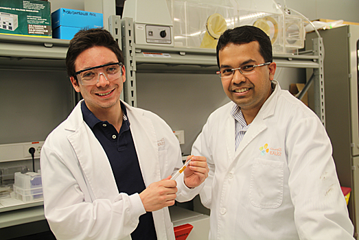
Galo Torres Seville, a KAUST Ph.D. student in Prof. Hussain's group and the first author of the paper, noted that "our objective as a research group is to find a bridge between portable and high-performance electronics that will one day allow us to perform very complex and time-consuming tasks with our portable devices. In our recent work, we have pushed inorganic electronics to a bending radius never shown before."
The transistor built by Prof. Hussain's team is constructed of a monocrystalline silicon-based substrate. Silicon is a material which, as the researchers state, is "the most highly used material in today's digital world…[M]ore than 90 percent of electronics are based on silicon micro- and nanofabrication processes."
However, there are some drawbacks to silicon electronics, including silicon's brittleness and lack of flexibility. To counter these problems, researchers have experimented with using polymer-based substrates, 2D single walled carbon nanotubes and 2D graphene to produce flexible electronics. But because of issues with these materials, Prof. Hussain's team has concentrated on a different fabrication process using silicon to make electronics flexible "without compromising cost, yield, performance and efficiency," Prof. Hussain said.
By following this process, which creates a network of trenches/holes, the researchers carried out an additional back-etch process from the back side of the substrate they used to ensure any holes/trenches would be eliminated in the peeled-off silicon fabric. They produced a FinFET, a nonplanar, multi-gated transistor constructed on a silicon-on-insulator (SOI) substrate.
The team's soft-etch back process thinned down the SOI wafer with the FinFETs on it. They also protected the device with a photoresist coating.
"Compared to the semiconductor industry's back grinding process, our process provides advantages from the perspective of its gentle manner to protect nano-scale devices and its thinning range," explained Prof. Hussain. "Our technique is a new way to replace back grinding for flexing traditional electronics and not compromise silicon's cost/yield advantage."
The researchers' method is also advantageous because it allows complete fabrication of the device prior to release, allowing standard processes to be kept in place to reduce constraints on design, etching, lithography and deposition techniques. In addition, because polymer substrates were not used, "thermal budget constraints are kept intact when compared to industry standard processes," they state.
With a final thickness of 50 µm, the device shows competitive electric behavior and bendability while "relying solely on mature micro- and nanofabrication techniques," note the researchers.
"Extreme bendability using only silicon is unique," said Prof. Hussain. "Flexible CMOS technology is imperative for advanced integrated electronic systems – our flexible FinFETs are taking us a step further in the direction of smart, interactive, 'live' and flexible technology. Future technology will only be limited by the range of applications that make use of silicon as a main material for device fabrication."
Torres Seville added that the group's process on this patented technology "will set a starting point towards the true integration of high-performance electronics on flexible substrates. We hope that through our work we can awaken the curiosity of researchers all around the world to pursue a common objective that will one day allow us to have devices that today we can only dream about."
By Caitlin Clark, KAUST News