High-resolution imaging of electron beam-sensitive materials

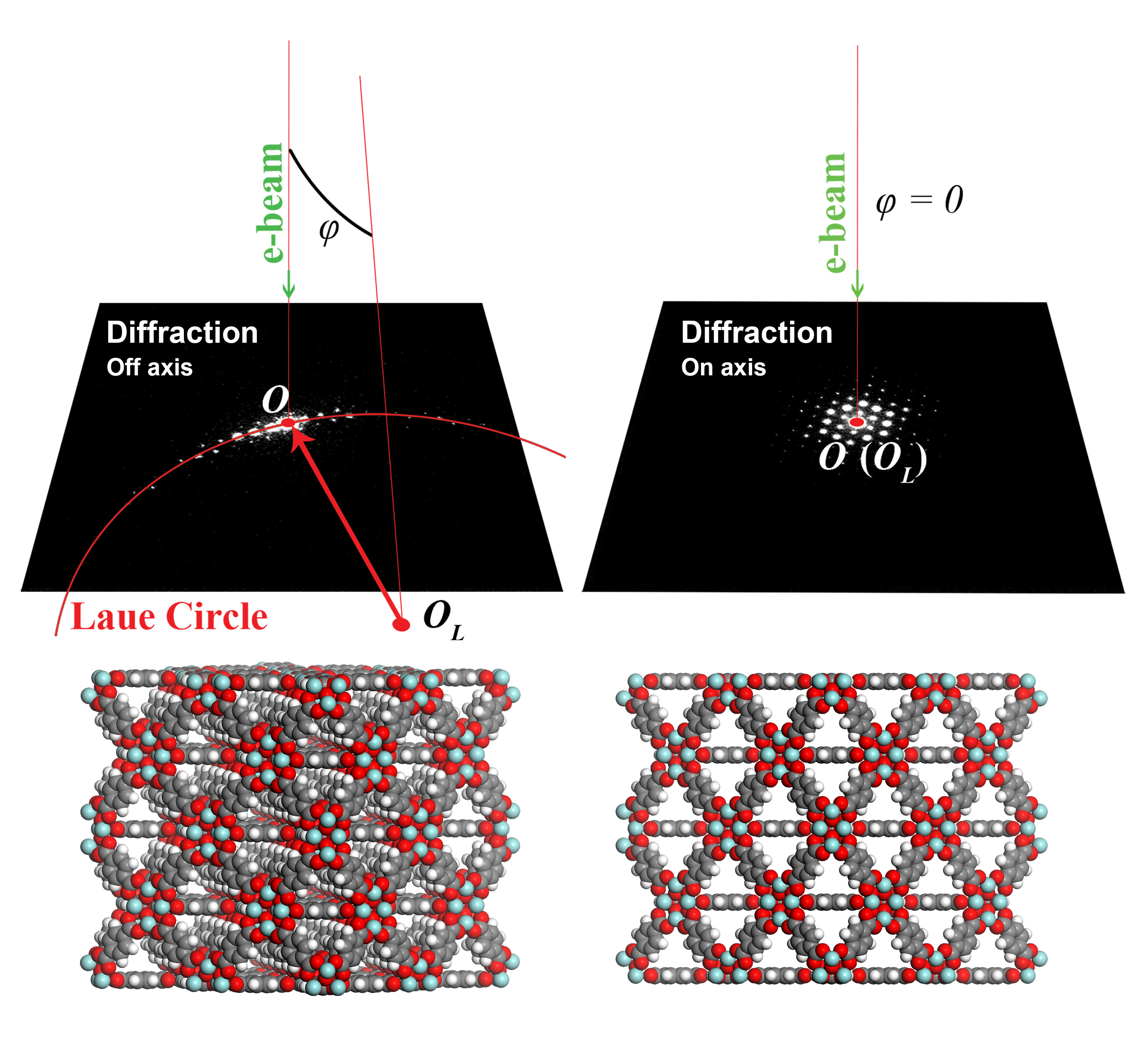
Off-axis and on-axis structure projections and the corresponding electron diffraction patterns.
-By Marian O'Neill, KAUST Core Labs
Staff members at KAUST devised a methodology for the procurement of atomically resolved images of beam-sensitive materials using transmission electron microscopy. Daliang Zhang, Rachid Sougrat and Kun Li from the KAUST Core Laboratories, in conjunction with Professor Yu Han and team members Yihan Zhu, Lingmei Liu, Xiangrong Ying and Chia-En Hsiung, published their findings in the current edition of Science.
"High-resolution imaging of electron beam-sensitive materials is one of the most difficult applications of transmission electron microscopy (TEM). The salient challenges are the acquisition of images using extremely low electron doses, the time-constraint inherent in the search for crystal zone axis prior to the sample being damaged, precise image alignment and the accurate determination of the defocus value," Han explained.

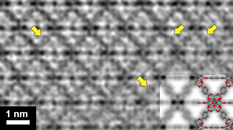
CTF-corrected High resolution TEM image from a MOF UiO-66 crystal. The benzene rings in the crystal are indicated by arrows. Overlays are simulated projected potential map and structural model for comparison.
Although high-resolution TEM (HRTEM) is a powerful tool for structure characterization, it is not easily applied to electron-beam sensitive materials such as MOFs, which require ultra-low electron doses to remain intact. The recent introduction of the direct electron detection cameras has provided scientists with the capability of realizing an image in ultra-low dose mode (only a few electrons per square angstrom), but the potential of such a camera in the HRTEM imaging of electron beam-sensitive materials is still limited by the inhibiting obstacles: sourcing a zone axis, aligning images and determining an accurate defocus value.

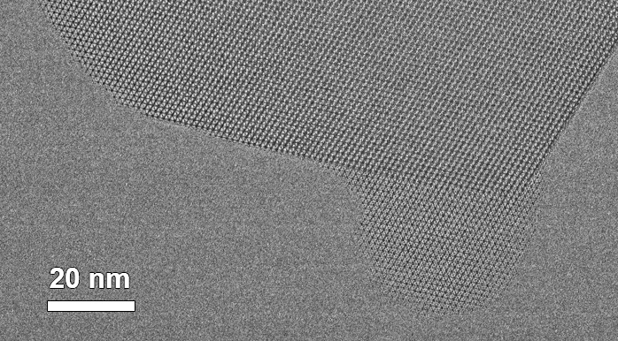
A high resolution TEM image of a truncated octahedral MOF UiO-66 crystal with <011> orientation.
These processes, which were developed at KAUST and incorporate two provisional patents, are not just limited to beam-sensitive materials. The method for zone axis alignment is also particularly pertinent for the aligning of nanosized crystals, and that for image alignment is generally applicable to noisy images with periodic features.

High resolution TEM images of MOF UiO-66 acquired from different crystallographic zone axes.