2D materials spur new electronic devices, circuits

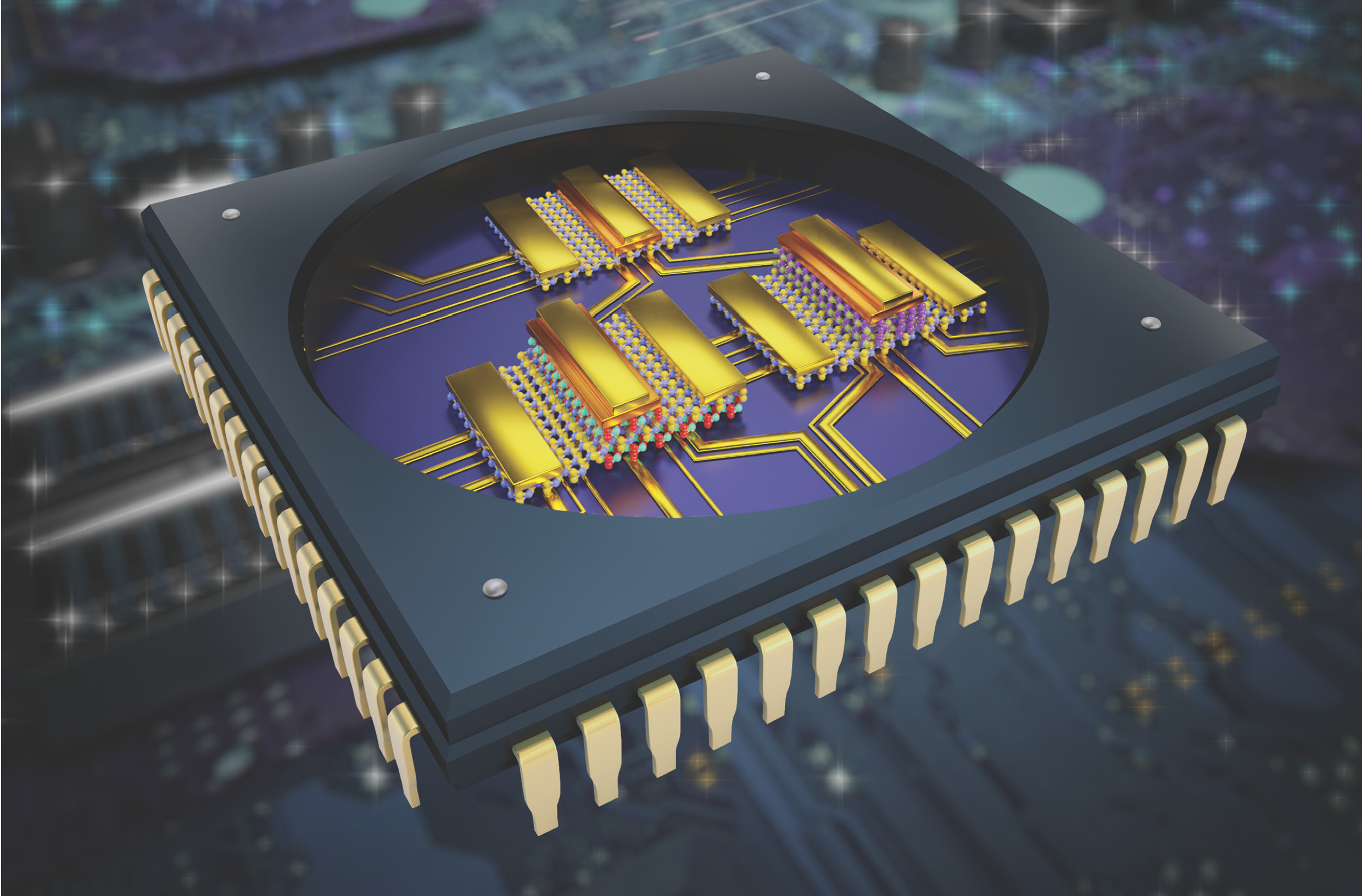
Illustration of a microchip containing field effect transistors made of two-dimensional materials. Graphic courtesy of Mario Lanza
The following editorial excerpt by KAUST Associate Professor of Material Science and Engineering Dr. Mario Lanza explores the state of two-dimensional materials in the creation of new concept devices. The full article, Electronic circuits made of 2D materials, written by Lanza and co-authored by Iuliana Radu, corporate researcher with Taiwan Semiconductor Manufacturing Company (TSMC) — the producer of 60% of the world's smallest microchips — appears in a special edition of the journal Advanced Materials (Adv. Mat. Vol. 34, 48/2022).
Two-dimensional (2D) layered materials may spawn a revolution in the field of solid-state micro/nano-electronic devices and circuits, owing to their outstanding electronic, physical, chemical and thermal properties. Some top scientists and companies suggest that 2D materials could be used to mitigate the limitations of silicon technologies, helping to extend the Moore's Law and create new concept devices beyond the complementary metal-oxide-semiconductor (CMOS) technology. Top microchip manufacturers like TSMC, Samsung, Intel and IBM and semiconductor research institutes like IMEC have already reported prototype field-effect transistors with 2D semiconducting channels. The International Roadmap for Devices and Systems (IRDS) — a document written by a world-class group of industry-led experts (who foreshadowed important developments in the past) — lists 2D materials as an option for commercial transistors and other beyond-CMOS devices around 2028.
The current status is that electronic devices made of 2D materials produced by mechanical exfoliation of small crystals have exhibited outstanding performance, such as transistors with 2D semiconducting channels that achieve high mobility, high current on/off ratio and low subthreshold swing. However, when nanosized devices are produced using scalable fabrication techniques, such as chemical vapour deposition (CVD), the performance remarkably degrades. For example, some of the best 2D-materials-based nanosized transistors fabricated by the industry show low mobility and high subthreshold swing, with very high device-to-device variability. The reason is the presence of local defects in the 2D materials and contamination. Interestingly, 2D materials show the promise for lower variability compared to silicon technology because of the amazing electrostatic control associated with these very thin channels.
By now, we have seen that 2D materials have started to be integrated in some commercial products that do not require a high integration density, such as sensors and speciality cameras. In these bigger devices, the effect of local defects in the 2D material is not so detrimental. However, commercial high-integration-density electronic circuits exploiting the properties of 2D materials are still a matter of research. Hopefully, as 2D materials start to enter in industrial laboratories with more controlled environments and materials processing (lithography, etching, deposition), the density of local defects and contamination can be reduced, and ultra-scaled devices might exhibit better performance and reliability.
In terms of exploratory research, the next steps to be taken in the field of 2D materials are to develop reliable device fabrication flows and to prototype electronic circuits capable of performing operations that single devices cannot do, such as logic gates using transistors or vector matrix multiplication using crossbar arrays of memristors (among many others).
In this special issue, Advanced Materials covers some of the most advanced knowledge in the field of 2D-materials-based electronic circuits, with 21 articles from leading experts that touch upon multiple aspects related to fabrication, characterization and modelling of electronic circuits made of 2D materials.
The first group of articles focuses on materials synthesis and their integration in micro/nano-electronic devices and circuits. The second, the development of electronic memories — one of the most important circuits in microelectronics, with a market that has reached a size of ~166.5 billion USD in 2021, only counting standalone memories. The third group of articles focuses on neuromorphic computation and development of artificial neural networks. This field is gaining a lot of attention because it can compute a lot of data in parallel to avoid the von Neuman bottleneck, sparing time and energy. The fourth focuses applications in different fields. The special issue finishes with three review articles sharing, from different perspectives, the overall vision of the field, the main challenges to overcome, and the possible strategies to follow in order to see 2D materials in commercial integrated circuits.
In addition to citing the research of Dr. Lanza, the special edition features research of KAUST Professors of Material Science and Engineering Dr. Xixiang Zhang and Dr. Husam Alshareef. Read more: Electronic circuits made of 2D materials.
Related links

